
Sign in
If you do not have an account, click Create AccountCreate Account
To better support our customers, we’ve launched an upgraded member platform with improved access and exclusive benefits.
Some items are no longer available. Your cart has been updated.


This discount code cannot be used in conjunction with other promotional or discounted offer.
Abstract
Introduction
1. Overall Circuit Structure
2. Detection Principle
3. Core Module Design
4. Capacitive Analog Signal Generation Model
5. Circuit Timing Simulation and Analysis
6. Conclusion
In response to the growing demand for high integration in specialized control chips for Vapes, this study designs a dedicated Vape control system comprising a conditioning amplification module, comparison processing module, temperature and current control module, atomizer wire drive module, LED drive module, over-temperature and over-current protection modules, and power supply module. For simulation purposes, a smoking signal model is constructed using Verilog-A. The circuit is implemented in a 0.18 μm BCD process and simulated using the Virtuoso Spectre simulator. Simulation results demonstrate that, at 27°C and a 3.7 V supply voltage, the system can process capacitance changes as small as 0.1 pF, enabling precise control of the atomizer wire and LED lights. When the system temperature exceeds 150°C or the atomizer wire current reaches 3.5 A, the over-temperature and over-current protection modules activate, halting operation of the atomizer wire and LED modules. This paper provides valuable reference for the advancement of Vape control circuit architectures.
Introduction
Currently, under the dual pressures of global tobacco control initiatives and public health concerns, traditional cigarettes face increasing restrictions, positioning Vapes as a market with immense potential. In China, Vape master control chips typically employ microcontrollers (Microprogrammed Control Units, MCUs) as the core, supplemented by a series of peripheral components to form the control system. This approach suffers from drawbacks such as circuit complexity, high power consumption, large area, and challenges in on-chip integration. References utilize digital control modules for signal management but require additional complex timing circuits. References adopt non-specialized control chips for Vape controllers. References use MCUs as control chips, incorporating numerous sensors for multifunctional control. With the rapid advancement of integrated circuit technology and increasing system integration levels, the aforementioned Vape control systems no longer align with contemporary technological trends. Therefore, this study designs a specialized Vape control circuit.
The overall block diagram of the specialized Vape control circuit is shown in Figure 1. The core circuit modules include the conditioning amplification module (AMP), comparison processing module (COMP), temperature and current control module (CTC), atomizer wire drive module (DRIVE), LED drive module (LED), over-temperature protection module (OTP), and over-current protection module (OCP). The AMP module handles amplification of the smoking signal. The COMP module compares and processes the voltage signal output from the AMP module. The CTC module controls input signals based on circuit temperature and atomizer wire (AT) current. The DRIVE module consists of multi-stage inverters with high drive capability and two high-voltage lateral double-diffused MOSFETs (LDMOS). It drives the atomizer wire AT and provides a current protection detection path. The LED module supplies appropriate current to drive the LED lights. The OCP module monitors current in the DRIVE module, while the OTP module monitors the overall circuit temperature. Voltage and current for the core modules are provided by the bandgap (BANDGAP) module and current bias (IBIAS) module, respectively. Under normal operation, the supply voltage is 3.7 V, and the bias currents from the IBIAS module are all 2 μA.
Figure 1. Circuit overall structure diagram
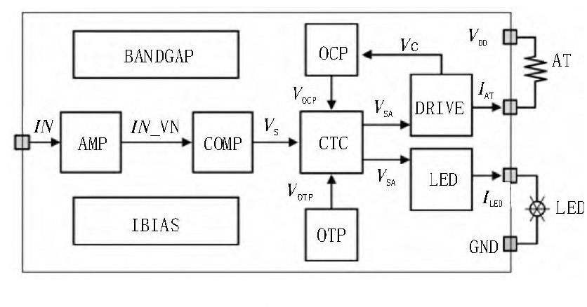
In practical circuits, the Vape mouthpiece is typically connected to an off-chip variable capacitor to generate a smoking action voltage signal. When the capacitor is exposed to varying air pressure, the distance between the plates changes, altering the capacitance value and thus the voltage across the capacitor. The input signal IN is the variable capacitor voltage. The IN signal enters the AMP module, where it is buffered and amplified, producing the amplified signal IN_VN, which is then fed into the COMP module. After comparison processing and state latching, the control signal Vs is output. The V_OTP signal from the OTP module and the V_OCP signal from the OCP module are transmitted to the CTC module. Only when both V_OCP and V_OTP are low can the Vs signal pass through the CTC module to output Vs_A. If either V_OCP or V_OTP is high, Vs cannot pass, resulting in Vs_A being low and halting circuit operation. When Vs_A is high, the DRIVE module conducts, providing a path for the atomizer wire AT, while the LED module conducts to drive the LED lights. The OCP module detects current in the DRIVE module; when the current in the protection detection path is excessive, the sampled voltage V_C rises above the set threshold, making V_OCP high. The OTP module detects the overall circuit temperature; when the temperature exceeds the threshold, V_OTP becomes high.
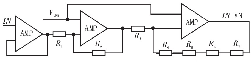
The circuit structure of the AMP module is illustrated in Figure 2, consisting of a voltage buffer follower cascaded with two inverting proportional amplifiers. The operational amplifiers used are low-offset, constant-transconductance, high-gain types. In the first-stage inverting proportional amplifier, the amplification ratio is controlled by resistors R1 and R2, fixed at 2 times. The second-stage inverting proportional amplifier uses resistors R3 to R7 of equal value, amplifying the input signal by 4 times. Overall, the AMP module amplifies the input signal by 8 times, fluctuating around 1.8 V.
Figure 2: Circuit structure of the conditioning amplifier module (AMP)
The circuit structure of the COMP module is shown in Figure 3, comprising two stages of basic amplification circuits. The first stage is a five-transistor differential amplifier formed by MOSFETs M1 to M6, and the second stage is a current sink inverter composed of M9 and M10. At the differential amplifier's input terminal VP, there are two input signals V_VP and VH_VP, controlled by M7 and M8, respectively, while the VN input connects to the conditioned amplified capacitance signal IN_VN. M11 and M12 are large-sized drive inverters, M13 to M16 form a latch with two inverters, M17 and M18 compose an inverter controlling VL signal, M19 and M20 compose an inverter controlling VH signal, and M21 to M24 form two inverters as output drive buffers. Metastability in comparators is a significant cause of conversion errors. When the instantaneous input signal is very close to the comparator's reference voltage, the output remains indeterminate for an extended period, leading to metastability, which requires longer stabilization times and affects circuit speed. The AMP module's output voltage fluctuates around 1.8 V, a non-fixed value, prone to metastability. Therefore, a latch composed of two inverters is added to lock the COMP output state, effectively eliminating metastability effects and improving comparator switching speed. The final buffer processes high and low levels from the previous stage, enhancing load drive capability at the output and overall comparator speed.
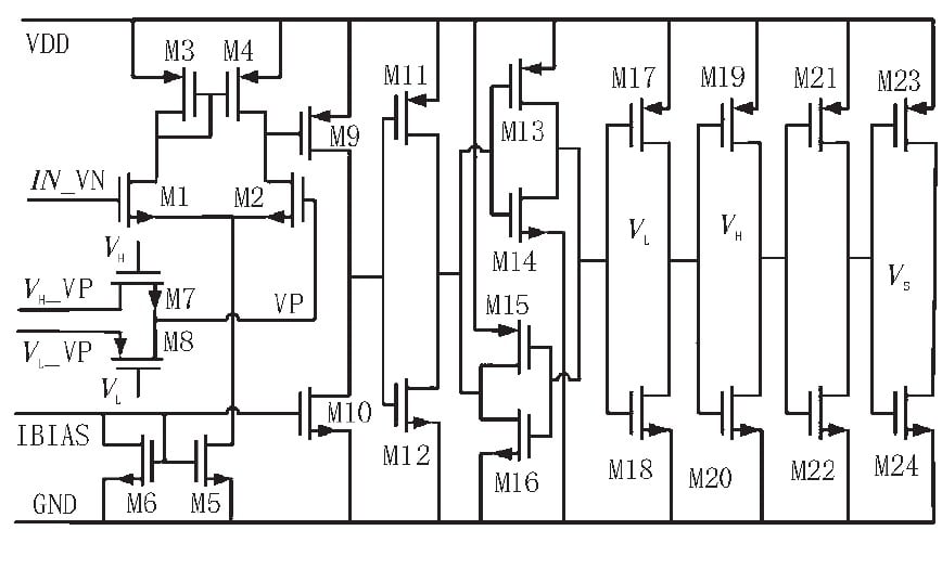
In the initial state, Vs is low, VL is high, VH is low, V_VP is 1.7 V, and IN_VN is above 1.7 V, keeping Vs low. When air pressure changes, capacitance varies, and IN_VN decreases. Below 1.7 V, Vs jumps, VH pulls high, VL low, and VH_VP becomes 1.9 V. As IN_VN continues changing, Vs remains high. When air pressure normalizes, capacitance returns to static, IN_VN rises, and above 1.9 V on the rising edge, Vs jumps low, VH pulls low, VL high, restoring the initial state.
The CTC module consists of a two-input XOR gate and drive inverters. The XOR gate inputs are V_OTP and V_OCP; if either is high, the output is high. The XOR output controls a buffer stage of two drive inverters to manage Vs conduction.
The LED drive module is a constant-current circuit comprising an operational amplifier and current mirror. The amplifier clamps the resistor terminal voltage to the input reference, generating a constant current mirrored to drive the LED lights.
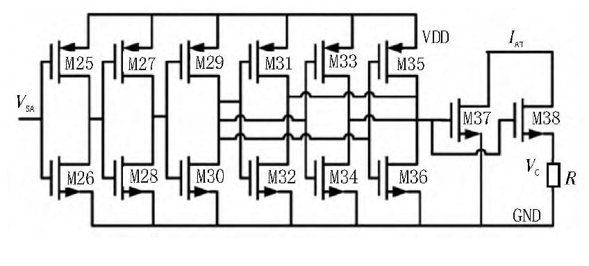
The DRIVE module employs electrothermal atomization, with its circuit structure shown in Figure 4. Vs_A connects via six inverters (M25 to M36), where the last three stages double in width-length ratio sequentially for current multiplication, providing sufficient drive for the power transistors M37 and M38, which are ultra-large width-length ratio LDMOS. M37 provides the high-current path for atomizer wire AT, while M38 is the sampling transistor in series with a voltage-dividing resistor, where V_C controls M37 current.
Figure 4 Schematic diagram of the atomizer drive module (DRIVE) circuit
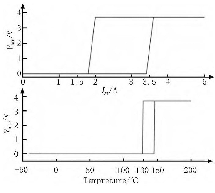
The OTP module comprises a simple hysteresis comparator and BJT transistor. Hysteresis is achieved via two switches to prevent frequent toggling near the threshold, ensuring circuit stability. Utilizing the negative temperature coefficient of PNP BJT, V_BE decreases with rising temperature and is compared to a reference. When temperature exceeds 150°C, V_BE drops, processed by the comparator to make V_OTP high, fed back to CTC. At 125°C, V_OTP becomes low.
The OCP module uses a simple hysteresis comparator. When current is excessive and sampled V_C exceeds the set value, V_OCP becomes high, fed back to CTC. Recovery occurs when current drops to 1.5 A.
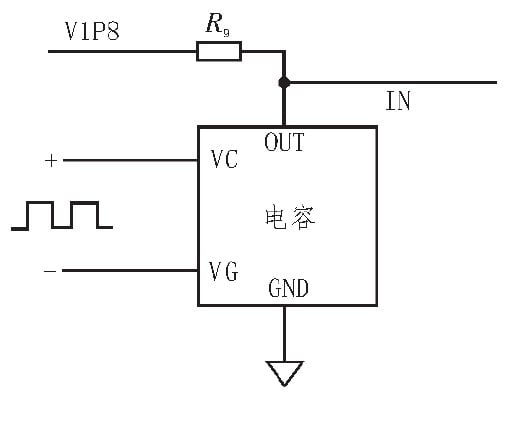
For simulation testing, the smoking signal capacitor is replaced by a Verilog-A equivalent capacitance module. The schematic is shown in Figure 5, with a mega-ohm resistor Rg in series connected to 1.8 V. Between inputs VC and VG, a square wave signal simulates smoking changes. When low, it represents no smoking (constant capacitance, unchanged IN). When high, it represents smoking (changing capacitance, varying IN). The Verilog-A implementation defines ports VC, VG, GND, OUT; uses case statements for capacitance states, if statements to judge VC-VG difference, selects cases, and differential equations for I-V characteristics. Operating at 1.8 V, static capacitance is 3.2 pF; dynamic is 3.3 pF under pressure change.
The core circuit is based on 0.18 μm BCD process, with 3.7 V supply. The Verilog-A model operates at 1.8 V, capacitance varying 3.2-3.3 pF. Simulations use Virtuoso Spectre. As shown in Figures 6 and 7, square wave input to the model produces IN spikes around 1.8 V with 20 mV amplitude. AMP amplifies by 8 times to 1.64-1.96 V as IN_VP. COMP processes quickly to Vs. Vs via CTC controls DRIVE and LED for normal AT and LED operation. Normally, OCP and OTP outputs are low. Waveforms in Figure 8 show high outputs when temperature >150°C or current >3.5 A. V_OTP drops low at 125°C; OCP at 2 A. If CTC detects any high, it cuts Vs, stopping operation.
Figure 6 AMP Amplification and COMP Output
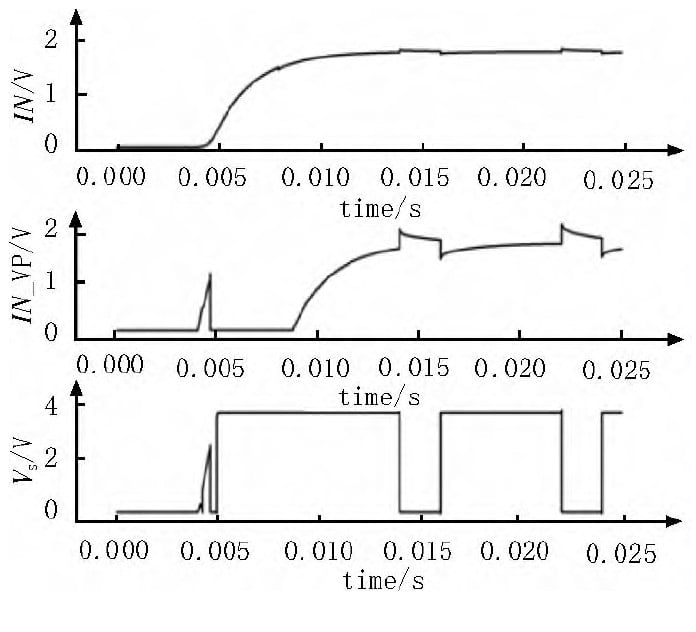
Figure 7 Atomizer Coil AT and LED Current
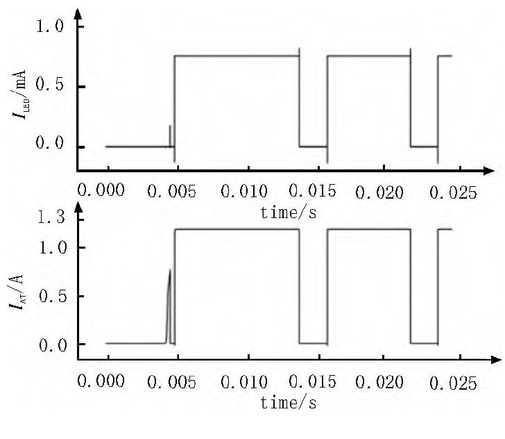
Figure 8 OCP and OTP Simulation Graphs
This study designs a specialized Vape control circuit system capable of accurately controlling the atomizer wire AT and LED lights, with over-temperature and over-current protection. The circuit is simple, requiring no timing generation. Implemented in 0.18 μm BCD process and simulated via Virtuoso Spectre, at 27°C and 3.7 V, it detects 0.1 pF capacitance minimum. Upon smoking signal, AT conducts and heats, LED brightens. Operation stops at >150°C or >3.5 A; resumes at <125°C and <2 A. Future enhancements could include digital control modules for additional modes and richer outputs.

Comment